Table of Contents
Overview:
While many people appreciate diamonds for their aesthetic appeal, they also significantly contribute to advanced technology. Color centers, imperfections in the diamond structure that can capture individual atoms or molecules, are an intriguing use. SiV centers are currently receiving much attention because of their potential in quantum technologies. Nevertheless, the task of producing SiV centers with optimal efficiency and accuracy continues to pose a significant problem. This paper examines the impact of sub-microsecond pulsed annealing treatments on the formation of SiV centers in diamonds. This treatment has the potential to facilitate progress in quantum computing and other related fields.
Comprehending SiV Centers in Diamond:
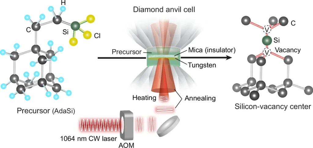
What is the precise definition of SiV centers? A SiV center is a point defect in a diamond crystal in which a silicon atom substitutes for a carbon atom, resulting in a neighboring vacancy. These centers’ distinctive optical and electronic characteristics, such as their ability to emit individual photons at a precise wavelength, make them highly valued. Applications such as quantum computing, where the ability to produce stable and consistent photons is essential, and quantum sensing, where they can detect magnetic and electric forces at the nanoscale, highly value these properties. Schematic illustration of pulsed laser-heating and annealing system.
Conventional Techniques for Generating SiV Centers:
Normal SiV center formation involves introducing silicon ions into a diamond lattice, followed by an annealing procedure to repair the damage from ion implantation. Typically, this process of annealing requires subjecting the diamond to elevated temperatures (exceeding 1000 °C) for prolonged durations. Despite its widespread use, this strategy carries significant drawbacks. Extended exposure to elevated temperatures can result in undesired alterations in the diamond’s composition, including the development of different sorts of flaws or even the transformation of the diamond into graphite, a form of carbon.
The Importance of Advanced Annealing Techniques:
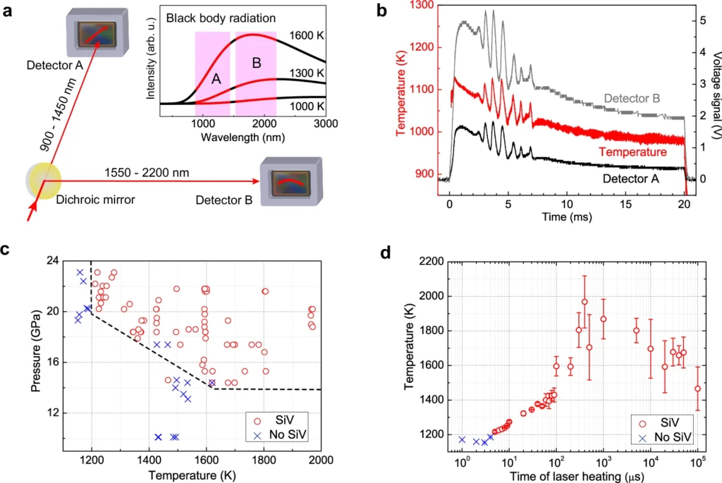
In light of these difficulties, there is an urgent requirement for more sophisticated annealing methods that can enhance the productivity and excellence of SiV centers while maintaining the integrity of the diamond. Conventional annealing methods are frequently characterized by sluggishness and a lack of precision, resulting in less-than-ideal outcomes. Obtaining consistent outcomes in annealing can be challenging due to the vast variation in temperature and time requirements. Sub-microsecond pulsed annealing is a method that provides a more precise and effective technique. In situ temperature measurement for laser-heated DAC.
What is Sub-μs Pulsed Annealing?
Sub-μs pulsed annealing refers to a process of rapidly heating and cooling a material within a time frame of less than one microsecond.
Sub-μs pulsed annealing is a method that utilizes brief and powerful bursts of heat to treat the diamond, with each burst lasting less than a microsecond. Pulsed annealing, in contrast to traditional annealing, applies energy in quick, concentrated pulses instead of uniformly heating the diamond for a long duration. By employing this technique, one may exert meticulous control over the annealing process, reducing the likelihood of causing harm to the diamond while efficiently rectifying any flaws.
We examine the process of creating SiV centers through sub-microsecond pulsed annealing:
However, what is the precise mechanism behind sub-microsecond pulsed annealing? The dynamics of temperature are the most important factor. Every pulse produces a momentary, powerful increase in temperature, which rapidly decreases before it can result in substantial harm to the diamond structure. The rapid thermal cycling increases the movement of silicon atoms inside the crystal structure, facilitating the creation of SiV centers while reducing the appearance of other imperfections. Furthermore, the short duration of the pulses helps to maintain the integrity of the diamond’s structure, thereby limiting the development of graphitic areas.
Design of an Experimental Configuration for Sub-microsecond Pulsed Annealing:
Specialized equipment is necessary to carry out sub-microsecond pulsed annealing. This comprises a pulsed laser or another high-intensity heat source that can emit energy in bursts lasting less than a microsecond, accompanied by accurate temperature control devices. The method begins with the introduction of silicon ions into the diamond, followed by a pulsed annealing treatment. In this context, important control parameters include the length and strength of the pulses, the total temperature of the diamond during treatment, and the surrounding pressure. We must precisely adjust these elements to achieve the intended results.
An Analysis of Sub-μs Pulsed Annealing vs. Conventional Techniques:
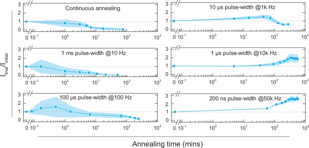
Sub-μs pulsed annealing provides numerous benefits in comparison to conventional annealing techniques. Firstly, it is significantly more effective at generating SiV centers. The quick pulses facilitate enhanced diffusion of silicon atoms, resulting in a greater density of SiV centers per unit area. Moreover, the brevity of the pulses greatly reduces the likelihood of harming the diamond or generating undesirable flaws. As a result, a diamond of superior grade with a reduced number of flaws is produced. Furthermore, sub-microsecond pulsed annealing is characterized by higher speed and greater energy efficiency, rendering it a more viable option for industrial applications. Sub-μs pulsed annealing measurement.
Case Studies and Research Findings:
The analysis focuses on specific instances and the results of scientific investigations.
Multiple investigations have shown that sub-microsecond pulsed annealing is highly effective in enhancing the formation of SiV centers. One study found that pulsed annealing increased the concentration of SiV centers by more than 50% compared to conventional techniques. A separate investigation indicated that diamonds subjected to pulsed annealing demonstrated a reduced presence of secondary flaws and improved overall crystal quality. The findings highlight the potential of sub-microsecond pulsed annealing to transform SiV center manufacturing.
We are optimizing the parameters for sub-microsecond pulsed annealing:
To fully reap the benefits of sub-microsecond pulsed annealing, it is critical to tune the process parameters. This entails adjusting the pulse duration to ensure that the temperature spikes are sufficient to create SiV centers without causing any harm. Furthermore, it is critical to properly control the temperature profile to avoid excessive or insufficient heating. Ensuring equilibrium between the energy input and output is crucial for attaining consistent outcomes. By fine-tuning these parameters, it is feasible to optimize the efficiency and quality of SiV center production.
There are obstacles and factors to consider:
Although sub-μs pulsed annealing offers numerous benefits, it also presents certain difficulties. An important concern is the exorbitant expense associated with the necessary equipment for the procedure, making it unaffordable for certain applications. Moreover, the process necessitates a considerable level of accuracy and mastery, rendering it more intricate to execute compared to conventional annealing methods. Additionally, there is a possibility of encountering unforeseen complications, such as the emergence of novel faults or the requirement for additional fine-tuning of the procedure. Further investigation is required to address these difficulties and fully exploit the capabilities of sub-microsecond pulsed annealing.
Applications Extending Beyond SiV Centers:
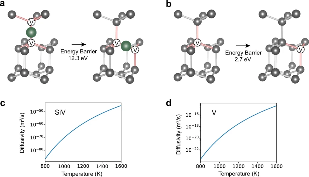
While the primary focus of this article is on the development of SiV centers, the techniques of sub-s pulsed annealing can also apply to other color centers in diamond, like nitrogen-vacancy (NV) centers, which hold significant importance for quantum applications. Furthermore, pulsed annealing has extensive applications in the fields of materials science and engineering, allowing for the repair or alteration of a diverse array of materials. The precise manipulation of the annealing process makes it a valuable asset in a variety of industrial and scientific contexts. Calculated diffusion pathways, energy barriers, and diffusivity for SiV and vacancy.
Environmental and economic consequences:
Sub-μs pulsed annealing is more energy-efficient than standard annealing procedures from an environmental standpoint. This is because it minimizes the total heat needed and shortens the treatment duration. This not only reduces energy consumption but also reduces the process’s carbon footprint. From an economic perspective, the improved efficiency and quality of SiV center manufacturing can result in long-term cost benefits, especially in large-scale industrial applications. Nevertheless, the upfront cost of equipment and the intricacy of the procedure may pose obstacles to widespread use.
Potential advancements in quantum technology:
In the future, the advancements in SiV center formation made possible by sub-μs pulsed annealing could have a crucial impact on the development of quantum technologies. The demand for high-quality SiV centers will inevitably rise as quantum computing and quantum sensing progress. Sub-microsecond pulsed annealing presents a possible approach to fulfill this requirement, offering a scalable and efficient technique for generating the high-grade diamonds necessary for these specific uses. Moreover, the incorporation of pulsed annealing into existing industrial manufacturing methods has the potential to catalyze advancements in quantum technology, hence creating promising prospects for the future.
In conclusion:
Sub-microsecond pulsed annealing is a significant breakthrough in diamond SiV center production. This technology enhances the efficiency and quality of SiV center manufacturing by providing accurate control over the annealing process while also reducing the potential for diamond damage. With ongoing research and technological advancement, sub-microsecond pulsed annealing has the potential to become a widely accepted technique in the field. This will accelerate the progress of quantum technologies and other related areas.
Frequently Asked Questions:
1). What distinguishes SiV centers as exceptional for quantum computing?
SiV centers provide consistent and dependable emission of individual photons at a certain wavelength, which is crucial for quantum computing applications that require accurate and dependable photon sources.
2). How does sub-microsecond pulsed annealing compare to other sophisticated techniques?
Instead of using traditional methods, sub-microsecond pulsed annealing is faster and more effective. It allows for better control of the annealing process and the creation of higher-quality SiV centers.
3). Is pulsed annealing applicable to different types of flaws in diamonds?
You can use pulsed annealing to repair defects in various color centers, such as nitrogen-vacancy (NV) centers, and in numerous other materials.
4). What are the primary obstacles to scaling up the implementation of sub-microsecond pulsed annealing?
The main obstacles include the exorbitant expense of equipment and the requirement for meticulous procedure regulation, which may complicate the implementation of large-scale operations.
5). What impact does the cost of sub-microsecond pulsed annealing have on its commercial feasibility?
Although the upfront cost of equipment may be substantial, the long-term benefits of improved efficiency and quality could potentially compensate for these expenses, making it a viable choice for industrial purposes.
For more chemistry blogs, visit chemistry Master